

The most stable microscope in the world
Making the most vibration-free, cryogenic scanning tunneling microscope in the world. A bold mission, but one that PhD candidate Irene Battisti successfully executed together with the Fine Mechanical Department. The new microscope might shed light on how unconventional superconductivity works. PhD Defence on 8 May.
Measuring near absolute zero
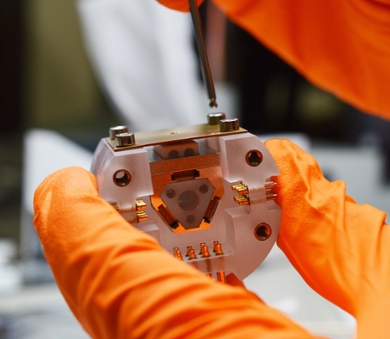
A scanning tunneling microscope (STM) is extremely delicate. A measuring needle, whose apex is atomically sharp, is brought to just a few angstroms away from the sample – only tenths of a nanometer. This is roughly the diameter of an atom, so the vibrations between the needle and the sample have to be extremely small. As a reference: the tip of Mount Everest would be allowed to vibrate less than the size of a bacterium. However, that’s not all. Battisti aimed to make a cryogenic microscope, with a temperature around 4 Kelvin – almost absolute zero. These ultralow temperatures are needed for spectroscopy, in order to visualize the electronic properties of materials down to the atomic scales. ‘This greatly complicates things, as the mechanics of regular STMs are not suited for such low temperatures’, Battisti explains. Therefore, she had to work with sapphire. ‘This material is not only expensive, but its toughness also makes it very difficult to process’, she says.
One of the most vibration-free places in the world
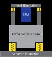
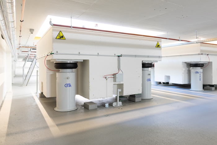
But stiff materials aren’t merely enough for creating such an extraordinary microscope; the location itself should be suitable as well. Luckily, the Ultramicroscopy Hall in the Gorlaeus Building has been designed to isolate vibration. According to the architect, it is one of the most vibration-free places in the world. This is achieved by a separate foundation, on which a concrete ‘island’ of 30 ton is suspended through springs, topped with a lead-filled table located on a second set of springs. Combine this with a unique design of the microscope and you’ve got the most stable cryogenic STM in the world.
The Fine Mechanical Department is essential
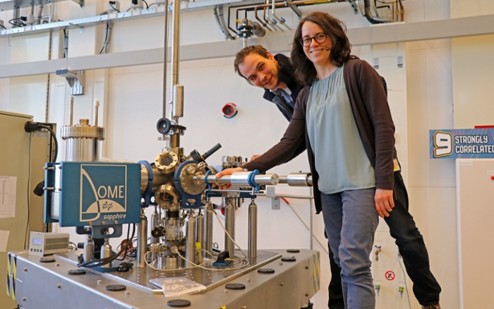
But why hasn’t this been done before? ‘Only recently, technology has developed enough to build this microscope. But more importantly, the Fine Mechanical Department (FMD) has crucial know-how and skills, which are quite unique in the world.’ Battisti worked closely together with Kees van Oosten and Gijsbert Verdoes from the FMD. She stresses that it was a real team effort. ‘For example, they are really part of our research group. And the fact that we are situated in the same building was really convenient and greatly improved the cooperation’, Battisti says.
Studying a mystery
The group of Milan Allan, which Battisti is part of, studies so-called quantum materials. These include high-temperature superconductors. ‘Normally, materials become superconducting below 4 Kelvin’, Battisti explains. ‘This requires liquid helium for cooling, which is very expensive. But some materials become superconducting at 100-150 Kelvin, which only requires the easy-accessible liquid nitrogen.’ However, how these high-temperature superconductors work remains a mystery, making it difficult to actually apply them in real-life. ‘Since I started my PhD, we have been working hard to understand this mystery, together with our colleagues from the Lorentz Institute. With this new STM, I hope to add some important pieces to the puzzle.’
Using waves to understand the material
‘We know that waves can interfere with each other’, says Battisti. ‘And by studying the interference pattern of waves, we can get to know something about the wavelength or the wave property. From quantum mechanics we know that we can see electrons as particles, but also as waves: the wave-particle duality. The experiments that we want to do are looking at the wave-like features of electrons. And with our new STM, we can visualize the interference between these electron waves on the surface of the material. From these patterns we can then extract properties of the electrons itself, and thereby properties of the material.’
Text: Bryce Benda
Header image: Interference of electron waves on the surface of a material, as measured with the scanning tunneling microscope. The waves form when electrons scatter off surface defects, which are visible as brighter features in the image.